Predicting the optical read-out of a qubit from first principles

Phonon-assisted luminescence is a key property of defect centers in semiconductors. It can be measured to perform the readout of the information stored in a quantum bit or used to detect temperature variations. The investigation of phonon-assisted luminescence is now generally carried out through models that incorporate restrictive assumptions and so fail to be predictive. The paper “Phonon-assisted luminescence in defect centers from many-body perturbation theory,” recently published in Physical Review Letters by researchers led by NCCR MARVEL’s Prof. Nicola Marzari and PhD student Francesco Libbi of EPFL’s Theory and Simulation of Materials laboratory, outlines a novel approach to predicting luminescence and studying exciton-phonon couplings with a many-body perturbation theory framework, an analysis that has never been performed for defect centers.

by Carey Sargent, EPFL, NCCR MARVEL

Quantum computers process and store information digitally, just like conventional computers. They do not, however, use switchable circuits that are either on or off—they rather use quantum physical systems that can adopt the two states simultaneously. The sort of system featuring this superposition of two states is known as a quantum bit, or qubit.

Though many systems have two precisely defined states that are subject to the rules of quantum physics, those intended for use as qubits must feature additional special properties. They must, for example, remain coherent for long enough to perform the quantum operations, be easy to control and efficiently readable. It must also be possible to switch qubits from on to off and back at extremely high speed. One approach that has gained a lot of attention is the idea of using electron spin as a qubit. It can only point “up” or “down” and so has exactly two states but can exist in a combination of the two.

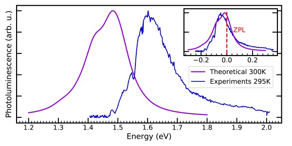
Figure 1: Theoretically predicted phonon-assisted luminescence (violet line), normalized and compared to experiments (blue line), at T=300K. The insets shows the theoretical and experimental curves after aligning the spectra. The agreement is very good for both the position of the peak and for the line shape. 

Manipulating the spin of individual electrons through microwaves and magnetic fields allows researchers to create superposition, the fundamental element of the qubit, as well as entanglement, a linking of the qubits that keeps them from acting independently. Creating qubits then means finding a spot in a material where the quantum properties of the electrons can be accessed and controlled.  

This is what has led, over the last decade, to a closer examination of defects. These spaces, where atoms are missing or misplaced in a material’s structure, can change how electrons move and, in some quantum materials, can trap electrons, allowing researchers to access and control spin. Such defects may therefore be an attractive option for making qubits for use in quantum computing, communication and sensing.  

In developing these possibilities however, it is critical to figure out how to determine the spin state of the defect center at a given moment. In this, the optical properties can play a major role:  spin-dependent luminescence can be used in the so-called readout, or deterministic measurement, of the quantum state of defect centers that respond to a technique called optically-detected magnetic resonance (ODMR).  

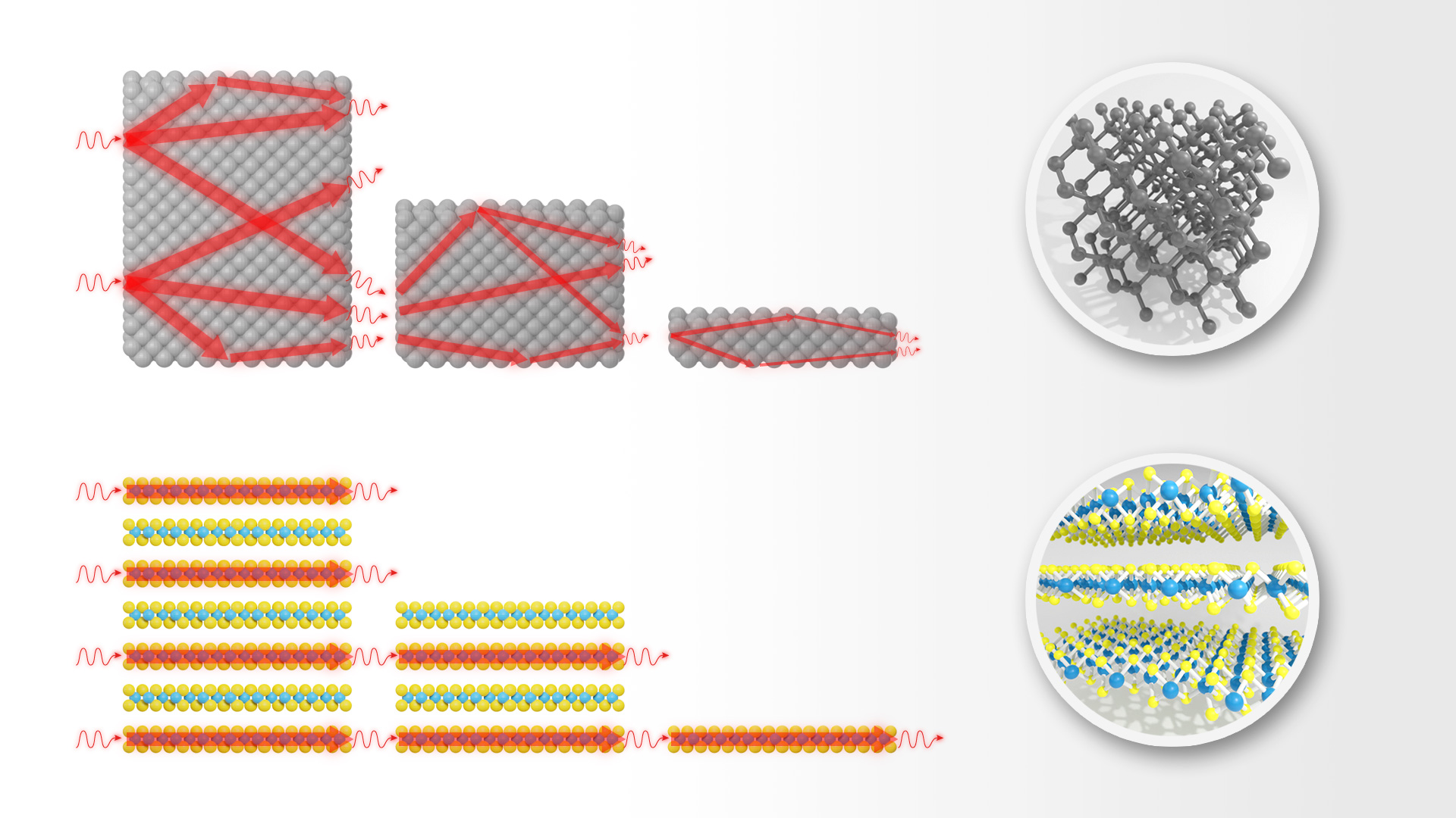
Defect centers in 2D hexagonal boron nitride (hBN) have recently gained attention due to features such as wide band gaps and low spin-orbit couplings that suggest advantages over existing 3D centers. Researchers have predicted that a negatively charged boron vacancy in the material is responsive to ODMR and emits in the infrared when stimulated with continuous green laser light, making it potentially useful in quantum computing. The peaks of the photoluminescence (PL) spectrum are also highly temperature dependent, meaning that they can be used to design sensitive thermometers.  

The photoluminescence of defect centers in semiconductors is often phonon-assisted because of the coupling of excitons with vibronic modes of the atoms around the defect. For this reason, this photoluminescence is usually studied using the Huang-Rhys model, which indicates the average phonons emitted during an electronic transition. This model is, however, based on certain restrictive hypotheses that limit its predictive power and it doesn’t support the interpretation of phonon-assisted luminescence in terms of coupling between excitons and phonons, an element that’s essential to understanding the phenomenon.

In the paper “Phonon-assisted luminescence in defect centers from many-body perturbation theory,” recently published in Physical Review Letters (PRL), researchers led by Professor Nicola Marzari and PhD student Francesco Libbi in the Laboratory of theory and simulation of materials at EPFL, took another approach. 

Many-body perturbation theory (MBPT), a means of accounting for electron correlation in calculating the probability of a transition between states of a continuous spectrum under the action of a constant perturbation has been used to study the optical properties of pristine hBN, allowing for the calculation of its phonon-assisted emission spectrum for both the bulk and the monolayer. The approach had never been used to study the luminescence of defect centers, however, because of the complexity and computational cost of the analyses. Now, in the PRL paper, it has been applied to predicting luminescence and studying exciton-phonon couplings of the negatively charged boron vacancy in 2D hBN.

Their simulations showed that the phonons are indeed largely responsible for the observed luminescence and that at low temperatures, the luminescence is determined by high frequency modes that are strongly coupled with excitons. Simulations also indicate that PL behavior that is very sensitive to temperature, suggesting that this defect can be used as a nanoscale thermometer, at least in a range of temperatures between 0 and 200 K.  

The agreement between theory and experiments is very good, the authors said, adding that they hope that their explanation of the photoluminescence mechanisms will further the technological integration of defect centers for quantum information and sensing.   

Reference:

F. Libbi, P. M. M. C. de Melo, Z. Zanolli, M. J. Verstraete, and N. Marzari,
Phonon-Assisted Luminescence in Defect Centers from Many-Body Perturbation Theory, 
Phys. Rev. Lett. 128, 167401

https://doi.org/10.1103/PhysRevLett.128.167401

Source: MARVEL highlights

Posted in 2D materials, ab initio, Boron Nitride BN, quantum bit qubit, quantum materials, Zeila | Tagged , | Leave a comment

Thin is cool: researchers unveil the excellent heat dissipation properties of layered semiconductors down to the monolayer

A study published in “Advanced Materials” reveals the thermal transport properties of ultrathin crystals of molybdenum diselenide, a two-dimensional material of the transition metal dichalcogenide (TMD) family. Outperforming silicon, TMD materials prove to be outstanding candidates for electronic and optoelectronic applications, such as flexible and wearable devices. This research, which involved researchers belonging to four ICN2 groups and from ICFO (Barcelona), Utrecht University (the Netherlands), the University of Liège (Belgium) and the Weizmann Institute of Science (Israel), was coordinated by ICN2 group leader Dr Klaas-Jan Tielrooij.

The increasing demand for extremely small components and devices has led scientists to search for new materials that could best meet these needs. Two-dimensional layered materials (2D materials) – which can be as thin as one or a few atomic layers and are strongly bonded only in the in-plane direction – have attracted the attention of both academia and industry, and do not cease to amaze with their peculiar and remarkable properties. Among them, transition metal dichalcogenides (TMDs) are promising for a variety of electronic, optoelectronic and photonic applications.

When it comes to the integration and miniaturization of devices, a key aspect to take into account is the thermal transport properties of materials: in most applications overheating is a crucial factor limiting performance and lifetime. Therefore, in order to take advantage of the electronic and optical properties of TMDs, a deep understanding and control of heat flow in these materials is required. In particular, comprehending the effects of crystal thickness – down to just one layer – and the environment on thermal transport are key to applications.

Influence of crystal thickness on thermal dissipation properties

A combined experimental and theoretical study recently published in Advanced Materials investigates the thermal conductivity of molybdenum diselenide (MoSe2), which is an archetypal TMD material. David Saleta Reig, PhD student and first author of the work explains: “We performed a systematic study of the effects of crystal thickness and surrounding environment on heat flow. This fills an important gap in the scientific literature about 2D materials.” Indeed, performing either reliable experimental studies or computer simulations of thermal transport over a broad range of thicknesses from bulk down to a single molecular monolayer is not an easy task. The authors of this research were able to overcome these challenges and produce protocols and results that are valid not only for the case study, MoSe2, but also for a broader range of 2D materials.

Ultrathin MoSe2 transports heat faster than ultrathin silicon

The experimental measurements, in combination with numerical simulations, led to a remarkable result: “We found that the in-plane thermal conductivity of the samples decreases only marginally when reducing the thickness of the crystal all the way to a monolayer with sub-nanometer thickness,” explains Sebin Varghese, PhD student and second author of the study. This behaviour originates from the layered nature of MoSe2 and sets TMD materials apart from non-layered semiconductors, such as the industry standard, silicon. In the latter, the thermal conductivity decreases dramatically when the thickness approaches the nanometer, due to increased scattering at the surface. This effect is much less significant in layered materials, such as MoSe2.

First principles thermal transport simulations reproduced the experimental results in an excellent way, and led to another surprising result: “For the thinnest films, the heat is carried by different phonon modes than for thicker ones,” says Dr Roberta Farris, postdoctoral researcher who developed and carried out the ab initio simulations. Finally, this study also clarifies the influence of the material’s environment on heat dissipation, demonstrating that ultrathin MoSe2 is able to dissipate heat very efficiently to surrounding air molecules.

Dr Klaas-Jan Tielrooij, who coordinated the work, comments: “This work shows that TMD crystals with (sub)nanometer thickness have the potential to outperform silicon films both in terms of electrical and thermal conductivity in this ultrathin limit”. These results thus demonstrate the excellent prospects of TMDs for applications that require thicknesses on the order of a few nanometers or less, for example in the case of flexible and wearable devices and nanoscale electronic components. “Of course it remains to be seen if TMDs will live up to their promises”, concludes Dr Tielrooij, “as there are many hurdles to overcome before these materials will be applied on an industrial scale. At least we now know that their thermal properties are – in principle – not a show-stopper.”

About the study

The authors of this study used the Raman thermometry technique to measure the thermal conductivity of a large set of suspended, crystalline, and clean MoSe2 crystals with systematically varied thickness, taking care to identify and suppress possible thickness-dependent artifacts. They compared the experimental results with ab initio simulations –based on density functional theory and Boltzmann transport theory— performed with the SIESTA method and software, which is particularly suitable for atomistic simulations with a large number of atoms.

This research, coordinated by Dr Klaas-Jan Tielrooij, leader of the ICN2 Ultrafast Dynamics in Nanoscale Systems Group, involved several ICN2 researchers and group leaders belonging to: the Phononic and Photonic Nanostructures Group, led by ICREA Prof. Clivia Sotomayor Torres, the Theory and Simulation Group, led by Prof. Pablo Ordejón, and the Physics and Engineering of Nanodevices Group, led by ICREA Prof. Sergio Valenzuela. Researchers ICFO (Barcelona), Utrecht University (the Netherlands) –with Prof. Zeila Zanolli, former member of Prof. Ordejón’s group—, the University of Liége (Belgium) –with Prof. Matthieu Verstraete, former visiting scientist at ICN2— and the Weizmann Institute of Science (Israel) were also involved.

Reference article:

David Saleta Reig, Sebin Varghese, Roberta Farris, Alexander Block, Jake D. Mehew, Olle Hellman, Paweł Woźniak, Marianna Sledzinska, Alexandros El Sachat, Emigdio Chávez-Ángel, Sergio O. Valenzuela, Niek F. van Hulst, Pablo Ordejón, Zeila Zanolli, Clivia M. Sotomayor Torres, Matthieu J. Verstraete, Klaas-Jan Tielrooij, Unraveling Heat Transport and Dissipation in Suspended MoSe2 from Bulk to Monolayer. Advanced Materials, January 2022. DOI: 10.1002/adma.202108352

Source: ICN2 news

Posted in Zeila | Leave a comment

Moiré materials: new understanding unlock the gateway to future nanoelectronics applications

A new research on electron conduction in double-wall carbon nanotubes finally offers an explanation for a long-ununderstood phenomenon about interlayer conductance and provides a predictive model to simulate the behaviour of such structures. A class of “switchable” nanotubes is also identified. This work, recently published in “Carbon”, was carried out in collaboration by members of the ICN2, Utrecht University and the University of Liège.

Quantum Conductance in double wall CNTs can proceed undisturbed and plateau to the conductance quantum (G0), partially transmitted, or completely blocked, depending on the spatial overlap of the two carbon nanotubes and their nature (chiral vector). Image: Damaso Torres, ICN2

The so-called moiré patterns are motifs that emerge when two repetitive structures are overlaid. This phenomenon is well known from computer or TV screens: when looking at a finely striped pattern, e.g. on a shirt, the stripes do not look evenly spaced and seem to bend in some areas. While undesirable in this case, the moiré effect can indeed be surprisingly useful in materials science. In fact, two atomically thin materials can be overlapped to create a new material, in which the atomic structures of the two produce a moiré pattern. Some of these moiré materials exhibit astonishing properties, drastically different from those of their components, which make them great candidates for application in novel nano-electronic devices.

Among many possible moiré materials, particularly interesting in this context are double-wall carbon nanotubes. They are made up of two cylinders, each composed of a single layer of carbon atoms arranged in a honeycomb structure, inserted one into the other. Since carbon nanotubes are mechanically ultra-strong and great electron conductors, their combination in such double-wall structure (exhibiting a moiré pattern) is very appealing. However, conduction between layers in double-wall carbon nanotubes has been little explored.

A study recently published in Carbon and led by Prof. Zeila Zanolli, from Utrecht University (The Netherlands), explores how electrons can move between the walls in moiré structures such as double-wall carbon nanotubes. Not only it provides a model to simulate such materials, but also sheds light on a hitherto unsolved mystery about quantized conduction. This research was carried out in collaboration with Nils Wittemeier, doctoral students at the ICN2, Prof. Pablo Ordejón, ICN2 Director and leader of the Theory and Simulation Group, and Prof. Matthieu J. Verstraete, from the University of Liège (Belgium).

The (until now) unsolved G0 mystery

Twenty-five years ago a group of researchers at the Georgia Institute of Technology measured electronic transport in multi-wall carbon nanotubes and stumbled upon an unexpected result. They observed a quantized conduction – which means that the conductance measured along the nanotube axis jumps from 0 to a constant value, instead of increasing gradually— which proved that the nanotubes are quantised conductors. But, according to commonly accepted theoretical predictions, they expected to measure a conductance of 4G0, where 2G0 is the contribution of each layer, i.e. the simple sum of the conductance of individual tubes. On the contrary, they observed a constant G0 value, even when overlapping more than two nanotubes.

Although proposals had been made earlier, the phenomenon remained unexplained until recently. The team of researchers led by Prof. Zanolli was able to prove that in some double-wall carbon nanotubes the quantum interaction between the two layers limits the conductance between them, so that it remains G0 (does not sum up to 4G0). Besides answering such a longstanding open question, this work provides more important contributions to this research field.

SIESTA method, analytical model and “switchable” nanotubes

The authors of this study performed atomistic simulations of nanotubes with up to 600 atoms using SIESTA, a first-principles materials simulation program developed by the ICN2 group led by Prof. Pablo Ordejón and one of the flagship codes of the MAX (MAterials design at the eXascale) European Centre of Excellence. They were able to devise a simple predictive model, which allowed simulating hundreds of nanostructures with up to 100,000 atoms, while retaining an accurate description of the electronic interaction between the two walls at the quantum level. This powerful tool is extremely valuable for studying and simulating moiré materials.

In addition, the researchers identified a class of nanotubes that show a behaviour similar to a light switch. In practice, by moving the inner wall slightly in and out of the outer wall, it is possible to change between an on-state –in which electrons can move between the walls— and an off-state –where they are blocked. The discovery of “switchable” nanotubes opens up new avenues for the development of innovative nanoelectronics devices.

Reference article:
N. Wittemeier, M. J. Verstraete, P. Ordejón, Z. Zanolli, Interference effects in one-dimensional moiré crystals, Carbon 186, 416 (2022) DOI: 10.1016/j.carbon.2021.10.028

Source: ICN2 News

Posted in Zeila | Leave a comment

Transition Metal Dichalcogenide monolayers investigated through Many-Body Perturbation Theory

Ultrathin layered 2D materials are next generation candidates for electronics and functional materials, but also superconductors and quantum computing. Their production quality has improved immensely but vacancies and impurities are found even in the best samples: it is critical to understand and quantify how defects change intrinsic properties, and use this knowledge to generate functionality.

A team of three researchers, composed by Pedro M. M. C. de Melo and Zeila Zanolli, respectively Postdoctoral Researcher and Associate Professor at the Condensed Matter and Interfaces group, University of Utrecht (NL) and Matthieu Jean Verstraete – Professor at the Physics Department of the Université de Liège (BE), employed the state of the art many-body perturbation theory to obtain the optical spectra resulting from intrinsic and extrinsic defects of the archetypical transition metal dichalcogenide (TMD) – WS2. In particular, ground-state calculations employed Density Functional Theory (DFT) using the Max flagship QuantumESPRESSO package, while excited state properties (GW energy corrections and Bethe-Salpeter absorption spectra) were computed using the flagship Yambo software package.

The work produced the first fully converged calculations of the optical spectrum of a full set of TMD defects. They consider the atomic vacancies of W and S and two representative substitutional defects. The simulated system sizes (70-80 atoms and large vacuum spacing around the TMD layer) allow to represent point defects realistically. They find that the vacancy and substitution defect classes have fundamentally different properties. The sulfur and tungsten vacancies show new exciton states below the pristine optical-gap, which makes them accessible by infrared lasers, while still being protected from thermal scattering. Particularly, the tungsten vacancy shows a larger set of extremely bright localised excitons. They show potential for device engineering as they would behave as photon emitters with multiple internal states, or even for multivalued quantum computing. The Mo and CH2 substitutional defects leave the full optical gap region available. These two substitutional defects offer potential for grafting and patterning in optical detectors.

In summary, metal vacancies show a richer set of polarised excitons than chalcogenide vacancies. In both cases excitons in the sub-optical-gap region are well localised near the vacancy site, making them good candidates for quantum dots, single photon emission, and qubits.

Large and pristine monolayers of transition metal dichalcogenides (TMDs) are difficult to manufacture, with most of them containing defects. Many-Body Perturbation Theory is used to demonstrate how different vacancies and substitutions can be spectrally identified in monolayer WS2, and might increase its functional potential, creating new quantum dots or adsorption sites.

Optical Signatures of Defect Centers in Transition Metal Dichalcogenide Monolayers, Pedro Miguel M. C. de Melo, Zeila Zanolli, Matthieu Jean Verstraete. Advanced Quantum Technologies (QUTE) 2000118 (2021) https://doi.org/10.1002/qute.202000118

Source: Material Design at the eXascale – MaX papers highlights

Posted in Zeila | Leave a comment

Science policy

‘The YAE is the perfect place to channel my ambitions’’

Doing science is one thing. Being involved in its policy making is quite another. However, the two are closely connected, and science policy can improve the quality of science. Italian researcher Zeila Zanolli was appointed as an Associate Professor in Quantum Chemical Modelling at Utrecht University last July. Despite many impressive achievements in her field of research, she still finds the time to fight for her beliefs about the conduct of science as a board member and treasurer of the Young Academy of Europe (YAE).

Concerns

Since she started her career as a researcher, Zeila Zanolli has been asking herself whether the scientific system is working as it should. Her concerns encompass many issues, ranging from Open Access publishing to the evaluation of excellence to the availability of permanent research positions, which she believes requires additional investments: “The grant system has become a lottery. We are wasting human capital. We train excellent scientists, depend on their work to advance science, but we can’t offer them permanent research jobs.”

Elected fellow

In 2016, Zanolli met Nicole Grobert at an academic convention. Grobert is Professor of Nanomaterials at the University of Oxford, and in 2016 she was serving as the Chair of the YAE, a group of young scientists active in science policy at the European level. She introduced Zanolli to the initiative. With Grobert’s nomination, Zanolli was elected as a Fellow of the YAE in 2017, and soon after she became board member and treasurer.

Channel ambitions

“For me, the YAE is the perfect place to channel my ambitions in terms of science policy”, Zanolli says. “We are in direct contact with organisations that have an advisory role to the European Commission, for example through Nicole Grobert, whom I mentioned before and who recently became Chair of the EC Group of Chief Scientific Advisors. Furthermore, we are well-informed about issues across Europe because of our close collaboration with young academies on a national level and other organisations, such as the Science Advice for Policy by European Academies (SAPEA), EuroDoc, and Marie Curie Alumni Association.”

Editorials and open letters

Recent YAE activities include an editorial in Nature about the protection of early-career researchers during the Covid-19 pandemic, a petition and an open letter to the Members of the European Parliament and national governments opposing budget cuts to Horizon Europe, and an online event to offer mentorship to young researchers from underrepresented countries to apply for an ERC Starting Grant.

YAE and Utrecht University

Another activity of the YAE, awarding the André Mischke Prize, is a token of the special connection between the YAE and Utrecht University. This prize for outstanding achievements in science policy is named after the late André Mischke, an Utrecht-based physicist and founding chair of the YAE. Zanolli regrets never having met Mischke but respects his legacy: “After he passed away, his wife made a donation to the YAE, which prompted us to rename the prize in her husband’s honour.”

Other current Utrecht based members of the YAE are Katell Laveant (board member), Lennard de Groot, and Oliver Plümper.

Source: Utrecht University

Posted in Zeila | Leave a comment

New theoretical studies of material properties as a function of thickness in chalcogenides

A study carried out by researchers from the Institute for Theoretical Solid State Physics in Aachen (Germany) and from the ICN2, and recently published in Advanced Materials Communications, reveals that materials of two subfamilies of chalcogenides show different dependence of their properties on slab thickness. This reflects on ferroelectric characteristics, which are relevant to their applications in information technology.

After the discovery of the striking properties of graphene, a material made up of a single layer of carbon atoms, 2D and few-layer materials have been studied with increasing interest due to their possible applications in various fields. What makes them special is the fact that their properties differ from those of the corresponding bulk materials, which are composed by more layers of the same kind. These differences are strictly connected with the kind of bonds that keep the layers together.

In order to better understand their characteristics and predict the behaviour of possible novel 2D and few-layer materials, theoretical simulations and computational resources are largely employed. Among the recently discovered families of 2D compounds, group IV chalcogenides (which are composed of an element of the IV group of the elements table, as Ge or Sn, and a chalcogen, as S, Se or Te) are particularly interesting since they exhibit remarkable electronic properties, including in-plane ferroelectric polarization.

In a work developed in close collaboration by Dr Ider Ronneberger, from the Institute for Theoretical Solid State Physics in Aachen (Germany), and Dr Zeila Zanolli, from the ICN2 Theory and Simulation group, and recently published in Advanced Materials Communications, the properties of a few compounds, representative of two subfamilies of group IV chalcogenides, have been investigated as a function of the slab thickness, using thin-film computational models. In particular, the study focused on analyzing, on one side, the behaviour of thin films of two selenides, GeSe and SnSe, which are held together by covalent bonds in their bulk state, and, on the other, that of thin films of two tellurides, GeTe and SnTe, which show an unconventional form of bonding, called metavalent bonding (MVB).

The simulations showed that, in the case of the selenides, bulk properties are recovered increasing the thickness of the material to just a few layers, while the structure of the tellurides thin films exhibits pronounced deviations from the bulk counterparts, even for thicknesses exceeding 18 bilayers (a bilayer is the “unit” of layers used in this research because more suitable to this study). As a result, these two groups of materials also present different ferroelectric properties, which are relevant to their possible applications, in particular to information technology.

This study provides crucial information about the characteristics and the bondings of few-layer structures from different families of compounds and allows predicting the behaviour of other 2D materials. Such knowledge is key to developing tools to tune materials properties according to the desired application.

Reference article:

Ronneberger I., Zanolli Z., Wuttig M. and Mazzarello R., Changes of Structure and Bonding with Thickness in Chalcogenide Thin Films, Adv. Mater. 2020. DOI: 10.1002/adma.202001033

Source: ICN2 news

Posted in Zeila | Tagged | Leave a comment

ICN2 doctoral student Nils Wittemeier honoured for his Master’s research

A Springorum Medal was awarded by the RWTH Aachen University to Nils Wittemeier for his Master’s thesis developed in collaboration with Dr Zeila Zanolli, of the ICN2 Theory and Simulation Group.

20191022_Nils_award

Nils Wittemeier, a PREBIST PhD student in the ICN2 Theory and Simulation Group, has been recently awarded the Springorum Medal by the RWTH Aachen University for his Master’s thesis on electronic and transport properties of multi-wall carbon nanotubes. His work was supervised by Dr Riccardo Mazzarello, from the RWTH Aachen University, and Dr Zeila Zanolli, senior researcher at the ICN2. It was also developed in collaboration with Prof. Philippe Lambin and Prof. Luc Henrard, of the University of Namur (Belgium), and Prof. Matthieu Verstraete, of the University of Liege (Belgium).

Nils performed simulations to help understand from a theoretical standpoint the results of some experiments on multi-wall carbon nanotubes, which had revealed a negative differential conductance. He performed first-principle calculations and set up a tight-binding model. His simulations reproduce general transport properties of carbon nanotubes but do not show any negative differential conductance, indicating that this phenomenon has not a purely electronic nature.

The Springorum Medal is named after Friedrich Springorum, co-founder of the Society of Friends of the Aachen University, as an expression of gratitude for his work for the Society and the University itself. This honour is awarded every year to the best graduates of each faculty.

Source: ICN2 news

Posted in Zeila | Leave a comment

Focus on Women in 2D Materials Science

A recent study led by Dr. Zeila Zanolli of the ICN2 Theory and Simulation group, on spectroscopic properties of few-layer tin chalcogenides, has been published on a special issue of the Journal of Physics Materials. This edition, called “Women’s Perspectives in Materials Science: 2D Materials”, will feature exclusively researches directed by female scientists, with the aim to highlight the excellent contributions of women to 2D Materials Science.

The Journal of Physics Materials has launched a special issue fully dedicated to the contributions of women to 2D Materials Science. The aim of this initiative is to give to distinguished female researchers recognition for their excellent work in this field and to support their career progression.  Despite the increasing involvement of women in important research projects, they are still underrepresented in leadership positions, in plenary and invited speakers lists at conferences, in journal editorial boards, and so on. “Women’s Perspectives in Materials Science: 2D Materials” will be one of a series of focus issues highlighting excellent contributions made by women in all the areas of advanced materials science.

This special edition dedicated to recent progress in synthesis, characterization and applications of 2D materials and structures features a new work led by Dr. Zeila Zanolli of the ICN2 Theory and Simulation group. This study, developed within a collaboration between the ICN2, the University of Liège (Belgium) – with an important contribution by Dr Antoine Dewandre –  and the University of Oxford (UK), aimed to investigate and model the structural, vibrational and electronic properties of tin chalcogenides (SnS and SnSe) and how their behaviour changes passing from a 3D to a 2D crystal and as a function of the number of layers of the structure.

Monochalcogenides as the compounds considered in this work have interesting properties, among which the fact that slabs of these materials act as semiconductors with low band gap and high mobility and are stable at room temperature. The reduction of the geometry of the crystal, of course, affects many of the characteristics of the material, thus it is necessary to investigate and describe them both theoretically and experimentally. For example, recent theoretical studies of electronic structure changes in few-layer Sn chalcogenides have shown a significant expansion of the band gap as the number of layers decreases.

Through calculation of electronic and phononic properties of slabs of mono- and few-layer Sn chalcogenide samples, the authors of this study identified spectroscopic signatures of 2D material thickness and propose several simple non-invasive techniques to discriminate different thickness samples. The outcome of this research provides useful tools for the experimental investigation of the properties of thin structures of these materials.

While Dr. Zanolli’s paper has already been published online (in open access), this special issue is not closed yet. In fact, contributions will be accepted until the end of January 2020 and published along the way. For more information, visit the journal website.


Article Reference:

Antoine Dewandre, Matthieu Jean Verstraete, Nicole Grobert and Zeila Zanolli, Spectroscopic properties of few-layer tin chalcogenides, Journal of Physics Materials, Women’s Perspectives in Materials Science: 2D Materials

DOI: https://doi.org/10.1088/2515-7639/ab3513

Acknowledgements:

Dr Zeila Zannolli’s reseach is funded by the Spanish Ministerio de Ciencia, Innovacion y Universidades, by the Spanish Agencia Estatal de Investigacion and the the Fondo Social Europeo, within the project: First principles engineering of novel nanomaterials for spintronics applications; grant number: RYC-2016-19344.

Image:

Representation of one of the surface vibration modes computed for the 4-layer slab of tin monosulfide (SnS). As the thickness of a material is reduced down to the nanoscale, prominent surface effects emerge due to the high surface-to-bulk ratio. Their signature can be identified and investigated using standard experimental technique, such as Raman vibrational spectroscopy. In thicker materials, the contribution of the inner atoms dominates the vibrational spectra and the surface vibrations cannot be detected. Frequency and amplitude of vibration are chosen to optimize the visualization.

Image Credits: The animation was produced by Antoine Dewandre using the Agate visualization tool developed by Jordan Bieder and available at: https://launchpad.net/~piti-diablotin/+archive/ubuntu/abiout

Source: ICN2 news

Posted in 2D materials, ab initio, chalcogenides, ETSF, nanoscience, publication, science, spectroscopy, Zeila | Tagged , , , , | Leave a comment

Happy International Graphene Day!

How would you celebrate a day dedicated to graphene reseearch? A nice short video on graphene-related research conducted at ICN2 will do the job!

Find me in the video at minute 1:27 !

…And here is the official ICN2 news:

The institution of an International Graphene Day, celebrated this year for the first time (today, June 6), was proposed by the China Innovation Alliance of the Graphene Industry (CGIA) to encourage researchers from all around the world, who work on this extraordinary material, to organize workshops, promotion events and communication activities.

A special event has been organized by CGIA in Beijing, involving both research institutions and industrial partners. The ICN2 is participating in the celebration with a short video offering a glimpse of the various research lines on graphene developed at our institute.

The video will also be broadcast at the GraphChina 2019 Conference, which will take place in October (19-21) in Xi’an, China.

Now, sit back and enjoy the viewing. Have a great International Graphene Day!

Source: ICN2 news

Posted in graphene, science dissemination, Zeila | Tagged , , | Comments Off on Happy International Graphene Day!

Dr Zeila Zanolli joins the Physics Editorial College of SciPost

SciPost is a complete scientific publication portal that offers two-way open access articles, i.e. free to publish and free to read. It is funded through donations and institutions, and is an important model in promoting open science.

20190528_ZANOLLI_Sci-Post

Dr Zeila Zanolli joined the ICN2 Theory and Simulation Group as a Ramón y Cajal research fellow in 2018. She has now joined the Physics Editorial College of SciPost, a portal with open, refereed and totally free scientific publications. She will be dealing with Condensed Matter Physics topics, including both theoretical and computational approaches.

SciPost is managed and run by professional scientists who aim to reform current practices in scientific publishing. As Dr Zanolli stresses, “we are encouraged to publish open access by the European Council. However, some journals charge 4000€ or even more to do so, when the real cost of a publication is calculated to be less than 400€ by SciPost”. Such high prices artificially inflate the cost of research, and make it impossible for investigators from low-resource groups to publish in certain journals (those with the highest impact factor).

Given that the quality of a group’s research is often measured by the impact factor of the journals in which it publishes, the system acts as a roadblock for these less resourced groups, and generates other undesired effects, such as overpublication or – even worse – scientific misconduct. SciPost wants to contribute to solve these problems by offering a two-way open access platform (no subscription fees, no author charges). Their costs are covered through donations from institutions which sponsor this initiative, such as Fonds zur Förderung der wissenschaftlichen Forschung (FWF Austrian Science Fund), OpenAIRE (Belgium), Max-Planck-Gesellschaft zur Förderung der Wissenschaften (Max Planck Society) or the Nederlandse Organisatie voor Wetenschappelijk Onderzoek (Netherlands Organisation for Scientific Research).

Dr Zanolli was elected to the board of Young Academy of Europe in November 2018. The YAE is a pan-European initiative of young scientists for networking, scientific exchange and science policy, and has recently backed Plan S for open access science. To Dr Zanolli, joining the SciPost Editorial College is a natural further commitment to open and sustainable science.

Source: ICN2 news

Posted in OpenScience, publication, science policy, Young Academy of Europe, Zeila | Tagged , , , | Leave a comment